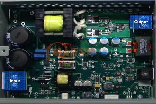
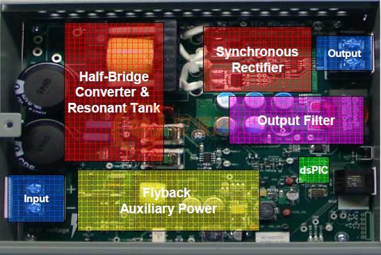
200W LLC Resonant Converter Reference Design (200 W谐振变换器参考设计)
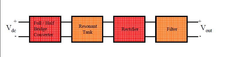
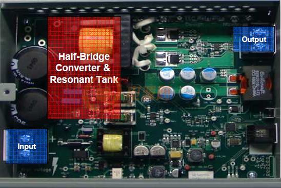
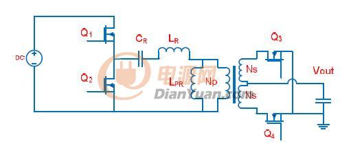
Half-Bridge Converter / Resonant tank
Next we will look at the operation of the half-bridge converter and the resonant tank.
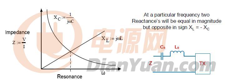
Half-Bridge Converter / Resonant Tank
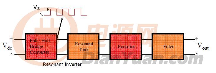
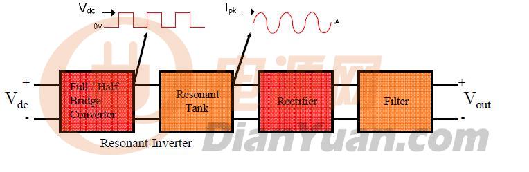
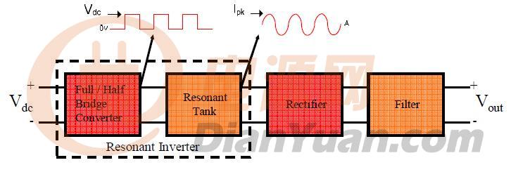
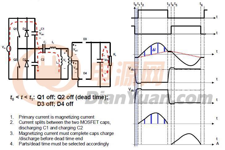
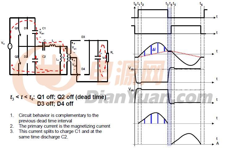
• Half-Bridge Converter generates a square wave with amplitude = VDC
and dc offset of VDC/2
• Resonant capacitor CR blocks dc component
• Resonant tank filters higher harmonics, essentially sinusoidal current is
allowed to flow
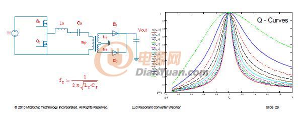
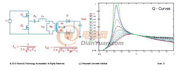
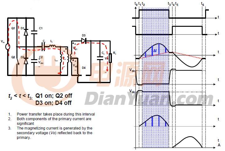
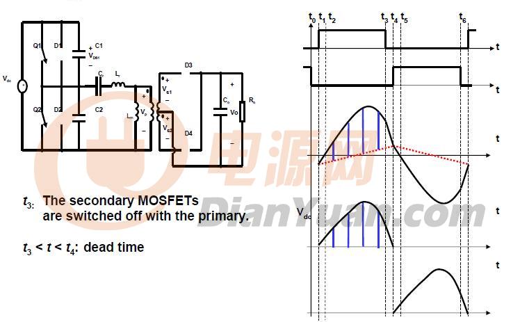
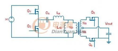
A circuit diagram of the half-bridge converter and the resonant tank is as
shown.
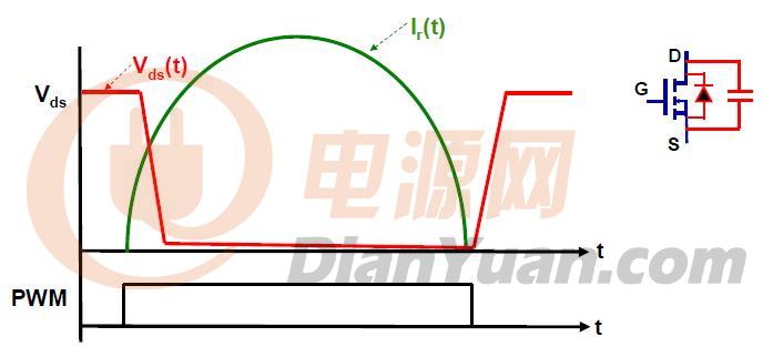
Two MOSFETs are connected in a bridge configuration and the resonant
tank is connected at the Half-Bridge point. The half-bridge converter is
configured in complementary mode with a fixed duty cycle (~50%) and with
some dead-time The dead-time serves two purposes: first, it prevents shootthrough
(both MOSFETs on at the same time), secondly, it is the time
interval used to charge/discharge the MOSFETs drain-to-source capacitance
used for zero voltage switching (as seen earlier in the presentation).
Because of the high switching frequencies MOSFETs are preferred over
IGBT’s.
The resonant capacitor blocks the DC component of the square wave,
producing a signal that is centered around 0v.
The resonant tank will filter the higher harmonics essentially only allowing
sinusoidal current to flow.
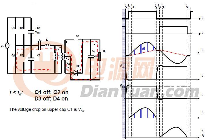
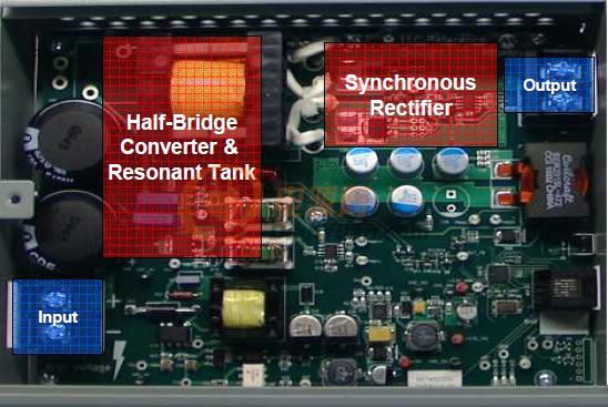
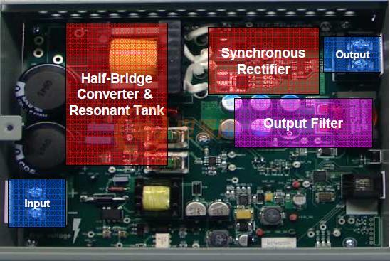
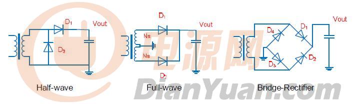
Synchronous Rectifier
Next lets look at the rectifier block found on the secondary side.
Types of Rectifiers
● Three topologies to consider:
- Half-wave rectifier
- Full-wave rectifier (center-tapped)
- Bridge rectifier – High output voltage low output
current
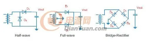
There are three different rectifier topologies to consider: Half-wave, Full-wave, and
Bridge Rectifier. As this application has a low output voltage (12V) and high output
current the bridge rectifier is not a suitable solution.
For this reference design we have used a Full-Wave rectifier but we have replaced
the Diodes with MOSFETs. This is more commonly known as synchronous
rectification. The MOSFETs switching losses and conduction losses are less then
that of the Diodes losses, which helps improve overall efficiency. The MOSFETs
have been placed on the low-side (ground reference) to reduce component count
and complexity.
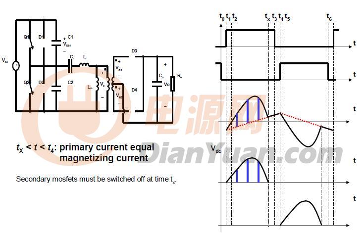
One thing to note is that now that we have added MOSFETs to the rectifier special
care must be taken to maintain Zero-Current Switching.
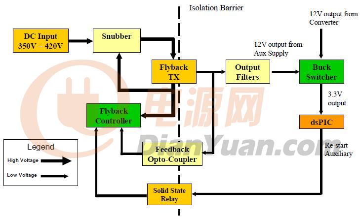
Flyback Auxiliary Power
Lets now look at the auxiliary flyback circuit.
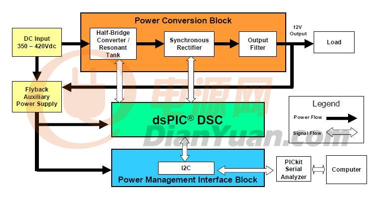
Auxiliary Power Block Diagram
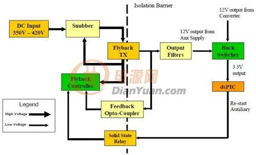
Here is a high-level block diagram of the auxiliary power section.
In this design we were targeting high efficiency and very low power at no/light load
operating conditions. To do this the auxiliary circuit has been designed with an auto
shut-off feature providing low stand-by power. The circuit also provides the ability to
restart the auxiliary circuit in the event of a fault condition.
Upon system start-up, the flyback converter provides power to the dsPIC. When the
dsPIC is up and running the output from the LLC converter (12V) will provide the
necessary power for the dsPIC, essentially powering itself.
Summary (概述)
Next, let us recap what we discussed on resonant converters.
● Resonant Converter Background
Information
● Different Resonant Converter Topologies
● LLC Resonant Converter Operation Modes
● Microchip’s 200W LLC Resonant Converter
We discussed the different resonant converter topologies,
operational waveforms of a LLC resonant converter, and Microchip’s 200W LLC
Resonant Converter Reference Design.
From our discussions we saw that the LLC resonant converter is a suitable DC-DC
converter for high-power applications with it’s high efficiency, high power density,
and its ability to operate over a wide input voltage range.
............................................................................ ............................................
资料全部上传完毕
原始资料: LLC Resonant Converter Reference Design using the dsPIC® DSC
最后再次感谢“uuniao”提供资料