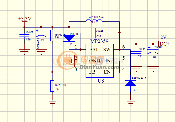
 MPS芯源降压芯片2359,没有3.3V输出,谁用过的?分析下
MPS芯源降压芯片2359,没有3.3V输出,谁用过的?分析下
全部回复(6)
正序查看
倒序查看
现在还没有回复呢,说说你的想法
很久没有上电源网了,随便刷一下看到MPS的帖子,怒答一发:
针对题主提出的这个问题,做如下建议:
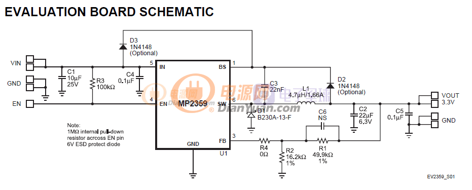
1.首先对照MPS给出的datasheet与demo资料核对一下电路有无问题;
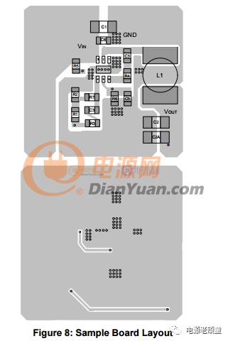
2.核对电路的layout有无问题
因MP2359与MP1470非常接近,所以拿MPS的MP1470为例,规格书中明确说了以下四条规则,严格遵循即可:
1) Keep the connection between the input ground and GND pin as short and wide as
possible.
2) Keep the connection between the input capacitor and IN pin as short and wide as possible.
3) Use short and direct feedback connections.Place the feedback resistors and compensation components as close to the chip as possible.
4) Route SW away from sensitive analog areas such as FB.
0
回复
提示
@湖之一二
很久没有上电源网了,随便刷一下看到MPS的帖子,怒答一发:针对题主提出的这个问题,做如下建议:1.首先对照MPS给出的datasheet与demo资料核对一下电路有无问题;2.核对电路的layout有无问题因MP2359与MP1470非常接近,所以拿MPS的MP1470为例,规格书中明确说了以下四条规则,严格遵循即可:1)KeeptheconnectionbetweentheinputgroundandGNDpinasshortandwideaspossible.2)KeeptheconnectionbetweentheinputcapacitorandINpinasshortandwideas possible.3)Useshortanddirectfeedbackconnections.Placethefeedbackresistorsandcompensationcomponentsasclosetothechipaspossible.4)RouteSWawayfromsensitiveanalogareassuchasFB. [图片]具体可以参考:电源老顽童写的《DC-DC的Layout经验总结》,可以私信我拿链接。
找到原因了,EN使能没有接100K电阻到VCC,
0
回复
提示